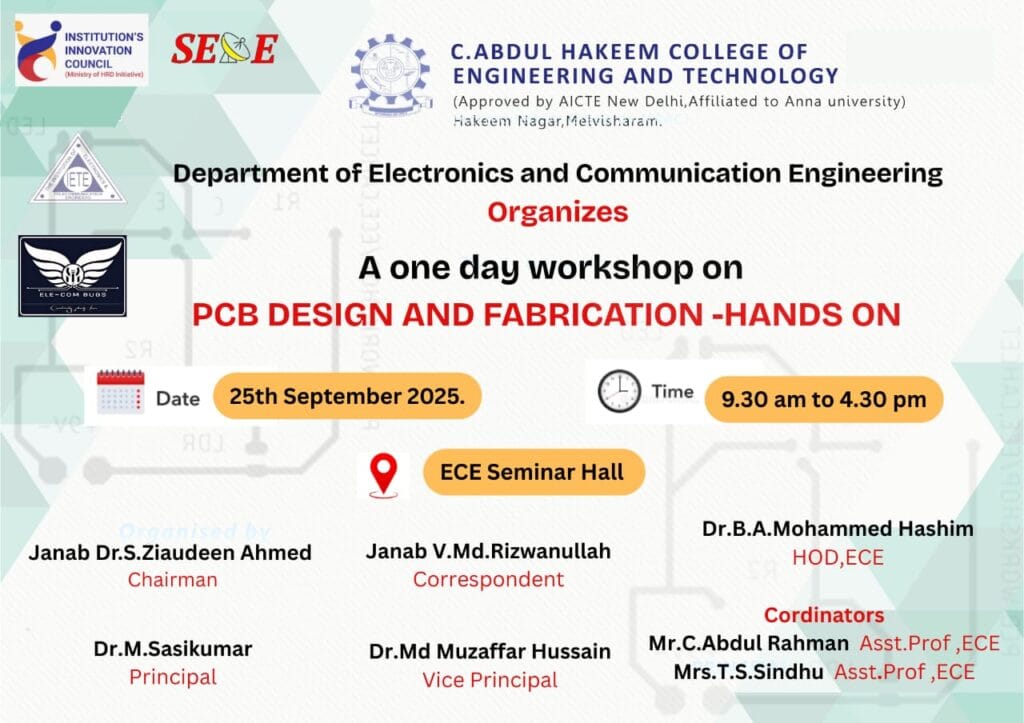
one-day hands-on workshop on PCB Design and Fabrication, organized by the Department of Electronics and Communication Engineering
📅 Date: 25th September 2025
🕒 Time: 9.30 am to 4.30 pm
📍 Venue: ECE Seminar Hall/ Networks Lab
🎯 “PCB Design and Fabrication – Hands-On”
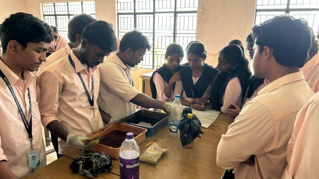
This workshop is designed to provide practical exposure to the entire process of PCB (Printed Circuit Board) design and fabrication, starting from schematic design to etching and testing the final board.
🧠 Key Topics Covered:
- Basics of PCB design principles
- Introduction to PCB design software (e.g., KiCad, Eagle, or Altium)
- Schematic entry and layout design
- Design Rule Check (DRC) and Gerber file generation
- Fabrication techniques: etching, drilling, and soldering
- Testing and troubleshooting the fabricated PCB
Benefits to Participants:
- Design and take home your own working PCB prototype
- Enhance your practical electronics and prototyping skills
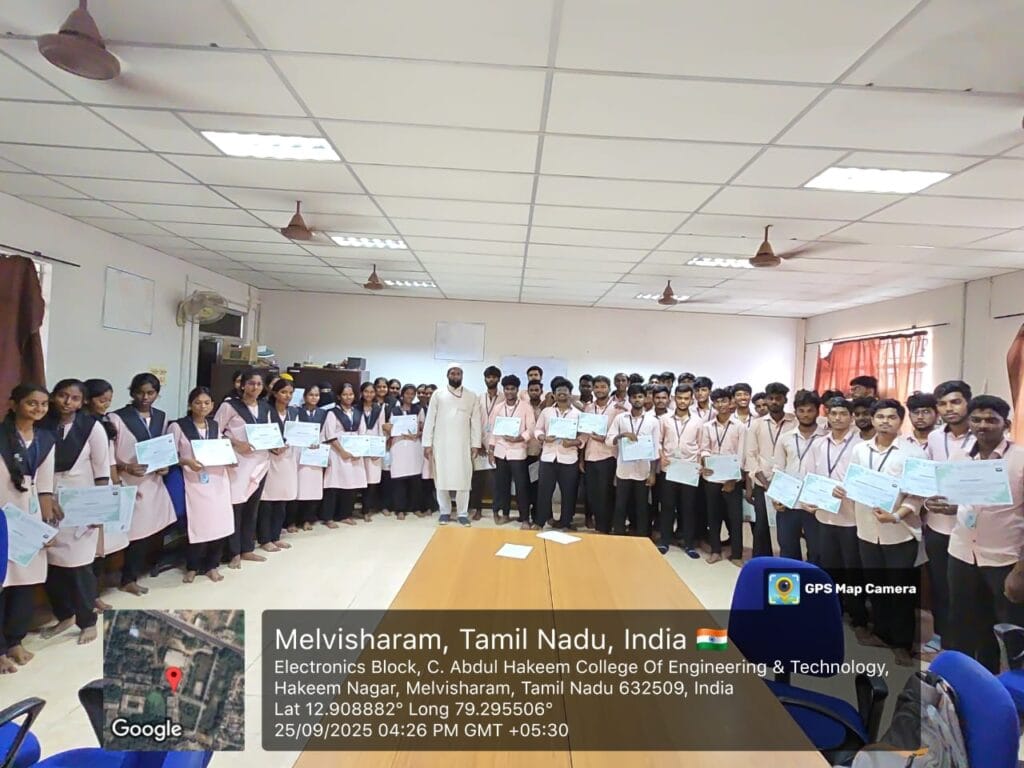
- Certificate of Participation from the ECE Department
- Ideal for students preparing for mini-projects, final-year projects, or DIY electronics
- Exposure to tools and workflows used in professional PCB manufacturing